Materials such as metals and semiconductors reduced to nano (one nanometer is one billionth of a meter) size particles exhibit different properties from those of a size visible to the naked eye. Nanoparticles of noble metals absorb light at a specific wavelength and show vivid colors. For example, COVID-19 test kits utilize gold nanoparticles that exhibit a red color if the test result is positive. Such nanoparticles, which respond to light waves (with wavelengths of several hundred nanometers), are called “nanoantennas.” Nanoantennas are analogous to antennas that emit and receive radio waves, which are electromagnetic waves with wavelengths longer than light waves. Nanoantenna particles should be suitable as biosensors and stable coloring materials.
Associate Professor SUGIMOTO Hiroshi of the Graduate School of Engineering discovered the forefront of this research field at Boston University, where he studied during his Doctoral Program. This experience led him to develop a unique manufacturing process for nanoantennas made from dielectric silicon. His project aims to create an international research platform for nanoantennas with Kobe University at its core so that silicon nanomaterials can be shared with research groups around the world. This project was awarded a Kobe University Strategic International Collaborative Research Grant*. We asked him about his career as a researcher, his research interests, and the aims of his international project.
At the forefront of research while studying abroad
What prompted you to research nanomaterials?
Prof. Sugimoto:
In high school, I was interested in chemistry, and as an undergraduate, I studied a wide range of subjects in electrical and electronic fields (including electric circuits, electromagnetism, physical properties, and quantum mechanics). I found the laboratory of Professor FUJII Minoru (Department of Electrical and Electronic Engineering, Graduate School of Engineering) fascinating and thanks to the early assignment system, I was able to become a member of the laboratory. In the laboratory, I conducted research on the physical properties of inorganic nanomaterials. I chose the same major in graduate school and conducted research on the development of novel nanoscale materials. The original goal was to control materials’ responses to light and find new functions by reducing the size to the nanoscale. I completed my Master’s degree six months early using an early completion system and continued on the Doctoral Program.
You were greatly influenced by your time at Boston University, where you studied abroad, right?
Prof. Sugimoto:
I studied at Boston University as a visiting researcher for about a year beginning in September 2014 when I was still a doctoral student. I wanted to conduct research in the field of photonics, which handles applied science of photons. Thus, I had to choose between the field of semiconductor physical properties, which I was familiar with, and the field of photonics. Because I always pick the more difficult option when wrestling with a decision, I opted for the field that I had no experience in. When I visited Boston, I found that the research projects reported in papers I had read before departing for the United States were already completed. Hence, subsequent research was already in progress. I realized that you never really know the latest research trends unless you directly stay there and get involved. I learned about the speediness of research activities and the importance of communication in research groups in the United States.
Could you describe your research in detail?
Prof. Sugimoto:
At Boston University, I studied metal nanoantennas in a field called “nanophotonics,” which aims to achieve advanced control of light by reducing materials to nanoscale . Some nano-sized metals change colors in response to certain wavelengths of light. For example, gold metal is originally gold in color, but nano-sized gold particles respond to and absorb green light, resulting in a red color because the particles do not absorb red light. I was working with metallic nanoparticle antennas to enhance or change the optical response of nearby materials. Fluorescence is a phenomenon in which a substance absorbs light and glows. If we can increase the intensity of that fluorescent light, we can apply such phenomenon to highly sensitive biological sensing and imaging with intensified fluorescent light of molecules.
Novel color inks being developed
After returning from Boston, you focused on silicon and developed a proprietary manufacturing method for silicon nanoantennas in 2017. Could you tell us about the development process?
Prof. Sugimoto:
Around 2017, research in nanophotonics focused on metal nanoparticles. However, some top-level groups were beginning to report that dielectrics with high refractive indexes showed a strong interaction with light. Such materials have potential to enhance light functioning as nanoantennas. Hence, we focused our attention on this and approached it from the standpoint of material development. In one sense, my research in Boston found the limitations of metals. Metals indeed enhance fluorescence but they also absorb light and convert it into heat. Dielectrics do not generate loss in resonance, therefore I thought they could enhance the performance.
I turned my attention to silicon because it was the material that I had been studying all along. Silicon is a dielectric and highly refractive material. A challenge in my doctorate research was silicon’s low ability to absorb light when reduced to nanoscale. However, once I learned about the difficulties presented by metals, which absorb light, silicon’s disadvantage of not absorbing light became an advantage. In short, a characteristic that was initially thought to be problematic can become very attractive depending on the purpose.
An international joint research project using silicon nanoantennas has begun. Could you tell us about the purpose and objectives of the project?
Prof. Sugimoto:
This project provides silicon nanoparticles developed with Prof. Fujii,who is also a participant, to various research groups. Providing ideal materials to members will enable the conduction of basic and applied research that was not previously possible. , We will create an international platform for nanoantennas by incorporating overseas researchers’ high-level measurement and application technologies. Through this project, researchers are challenged to discover new phenomena, verify their applicability, and develop applications collaboratively. Based on an original idea from an overseas researcher, we recently started to research applying nanoantennas to an optical device in a way that we hadn’t considered before. We aim to establish a bilateral international consortium with more than ten research institutes in Europe and the United States that we are already conducting joint research projects with.

What kind of research results do you expect?
Prof. Sugimoto:
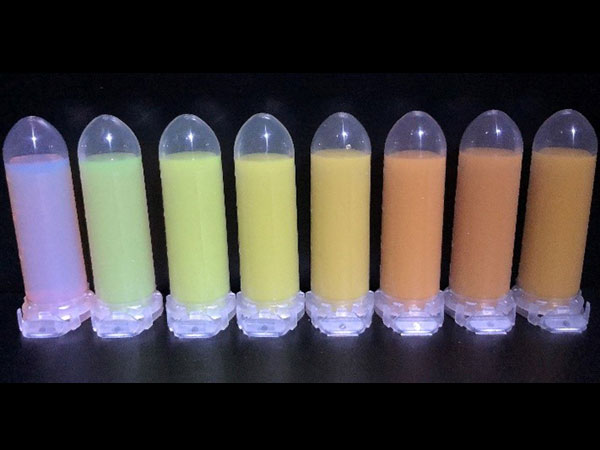
As for basic research, I am expecting many outcomes from our initial experimental studies on silicon nanoantennas. These include the experimental demonstration of physical phenomena that have been theoretically predicted. . One target of applied research is to advance sensors in the field of biosensing. The detection of a particular protein is determined from the response when light hits it. The speed and accuracy of the detection depend on the amount of protein required for precise detection. The smaller the necessary quantity, the faster the detection. Currently, a COVID-19 test kit requires a certain number of viruses to produce a red-colored line because many gold nanoparticles need to be adsorbed to produce the red color. However, it could be possible to achieve a more sensitive level of detection by using different type of fluorescent sensor, which has an enhanced light-responding property mediated by nanoantennas.
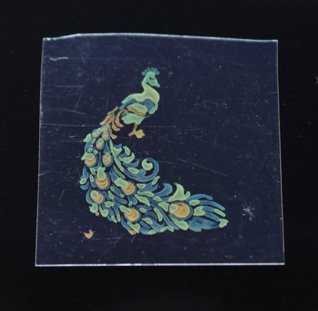
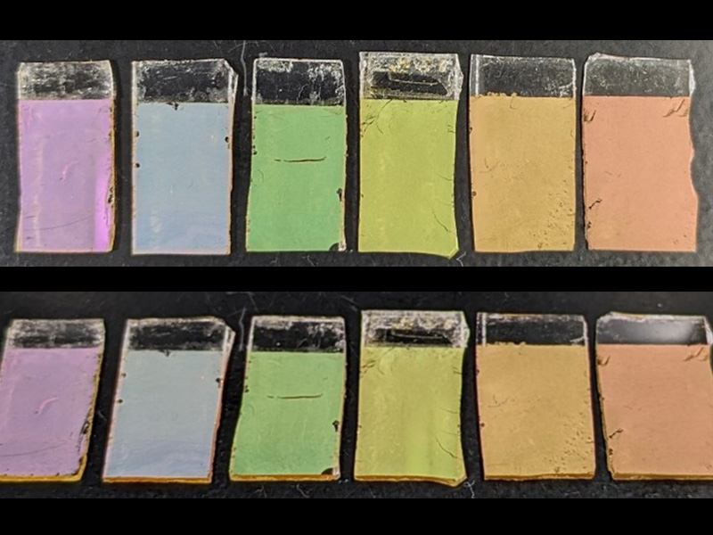
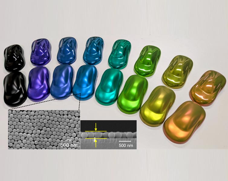
Outside of this project, we are also looking forward to further applications of nanoparticles in color inks and other materials. The resonant wavelength of silicon nanoparticles depends on their size. For example, at one size, they strongly scatter blue light, but at another, they strongly scatter green. Different colors are obtained by altering the particle size, which means that the currently used organic paints can be replaced with inorganic, stable ones. Such paints, which use a phenomenon called “structural coloration,” are being developed for use as printable inks. Special applications are expected; these include applications that freely control color and cut UV rays with a thin film such as anti-counterfeiting, semi-permanent coloring that does not fade, and cosmetic applications. We are planning to scale this up for commercial mass production. In this way, we continue to conduct research, including industry–academia collaborations, not only for generating academic results but also for realizing practical applications.
Resume
| April 2012 – September 2013 | Department of Electrical and Electronic Engineering, Graduate School of Engineering, Kobe University. Completed the Master’s Program in one and a half years. |
| October 2013 – March 2016 | Completed the Doctoral Program at the same Department and earned a doctoral degree. |
| October 2016 – September 2022 | Assistant Professor, Graduate School of Engineering, Kobe University |
| October 2022 – Current | Associate Professor, Graduate School of Engineering (Outstanding Associate Professor, Kobe University Institute for Advanced Study). |
*Note
- Strategic International Collaborative Research Grant | Kobe University
Associate Professor Sugimoto’s project has been approved as a Type B project under the Kobe University Strategic International Collaborative Research Grant program. - Kobe University’s research highlights:
International consortium on ‘Mie-tronics’: a new emerging field of nanophotonics