Nanophotonics is a research field in which light is freely controlled by nanosized structures even smaller than the wavelengths of light itself. A Kobe University research group developed a nanoparticle made from silicon called a “nano-antenna” and provided this nanomaterial to research institutes both in Japan and overseas, engaging in international joint research projects for the past three years. This research then developed into an international research platform with Kobe University at its core and is expected to be applied to a wide variety of fields, from next-generation optical information communications technology to life sciences. We asked Associate Professor SUGIMOTO Hiroshi of the Graduate School of Engineering, an expert at the forefront of his field, about the results of the past three years and his thoughts on potential future developments.
A new material that only reacts to specific wavelengths
Developing this new optical antenna from silicon and shifting to international joint research three years ago has breathed new life into the field of nanophotonics.
Sugimoto:
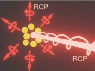
If you turn matter like metals or semiconductors nanosized (1 nanometer is 1 billionth of a meter), you will begin to see properties that differ from what we’re used to seeing. For instance, to our eyes, gold has a metallic luster in a yellow hue and thus looks “golden.” But if you make that gold nanosized, the green wavelengths of light (light waves) get absorbed and the red wavelengths are reflected, which would then make it look red to our eyes. These nanoparticles that respond to specific light waves were named “nano-antennas” as an analogy to the more conventional antennas that regulate radio waves. The antennas made up of connected pipes that we see on the tops of buildings are as big as they are because they need to receive electromagnetic waves with wavelengths that range from a few dozen centimeters to one meter. On the other hand, since nano-antennas regulate electromagnetic waves with short wavelengths, specifically those with just a few hundred nanometers, they require antenna technology that is the same size as those wavelengths or smaller, and are thus sometimes called “optical antennas.”
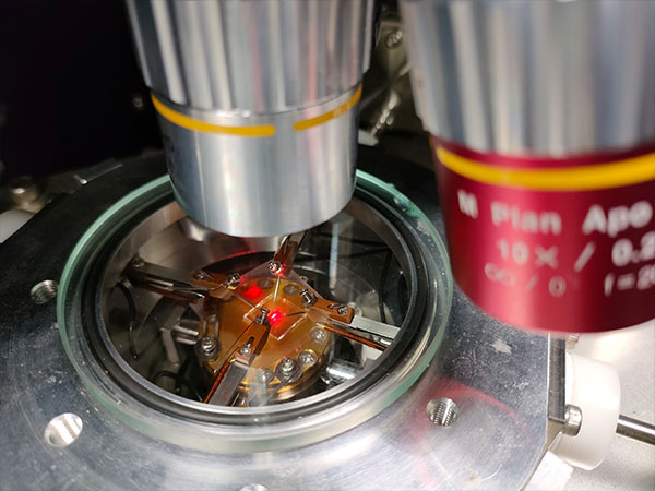
Various materials and structures have been considered for use in nano-antennas, but in 2017, a Kobe University research group developed one using silicon, which is widely used in semiconductors all over the world. Depending on the size of their particles, silicon nano-antennas react to specific colors or wavelengths of light, allowing wavelengths of all other colors to pass through without being absorbed. This phenomenon of acting in response to a certain wavelength is called “resonance.” Simply by changing the particle size of silicon by a few nanometers, almost every color from blue to red can be produced. One advantage that silicon has over metallic nanoparticles is that none of the light absorbed by the silicon will be converted to heat.
Expansion to 10 groups at research institutes in Europe and North America
You’ve provided your silicon nanomaterials to research institutes in Europe and North America for carrying out research.
Sugimoto:
As of May of this year, we are performing joint research with around 10 research groups at universities such as Stanford University (USA) and the University of Fribourg (Switzerland). Of the top 10% of research papers in their respective fields, only 2% are from Japanese universities, so it’s natural for the focus to shift overseas. For instance, if a particular research group is recognized as being at the forefront of its field, one would choose to perform world-class research with that group regardless of whether the group is from Japan or overseas.
My research group doesn’t just provide nanoparticle materials and that’s the end of it; everything we do is for joint research. Depending on the results of whomever I’m working with, I sometimes provide feedback on how to solve issues on the materials side of things. As someone in optics and physics, this allows me to get insights into any issues they may be having with their measurements or applications, rather than just simply provide them with the materials.
Have you learned anything new since you began providing these materials?
Sugimoto:
On top of the uses for these materials that I had initially hypothesized, research institutes that apply to perform joint research have also submitted ideas that we had not previously thought of. These ideas were published in journals and presented at conferences of completely different research fields from ours, it was one surprise after another.
For instance, we perform joint research with research groups in Europe and North America on topics such as optical tweezers, which capture biological matter with light, and using silicon nanoparticles in transparent solar batteries. Being able to discover these kinds of applications and surprising functions that we would have never thought of provides a huge significance to joint research.
Exchange with human resources overseas and increased funding
Have there been any cases of research not going well?
Sugimoto:
Of course, there are times when things don’t go quite as we predict. Sometimes things don’t go the way we had initially intended, and there have been cases in the past in which projects were ended because they were short-staffed, since postdocs and doctoral researchers overseas (who bear the research duties) have their own respective full-time work.
There have also been cases where we’ve shared personnel among our research groups after identifying issues and went on to produce results. A doctoral student staying at a collaborating institute utilized the knowledge they acquired in the lab at Kobe University to solve issues, eventually getting their work published in a distinguished journal. This backup was only possible because the student regularly used these nanomaterials and was familiar with their characteristics.
In my research group, it is of the highest priority to provide the greatest support possible to students and early-career researchers in order to nurture them into talent that can thrive on the world stage. The more you invest into that talent, not only will the university better fulfill its duties as an educational institution, but those investments will also pay dividends in the form of research results. I’d like to have the experience of going overseas serve as a foundation for students in the doctoral program.
In fact, we’ve seen a huge increase in students who advance to the doctoral program for that very reason. There are currently four students in the doctoral program, but there’s been an increase in the number of students considering advancing to the doctoral program from early on in their master’s studies.
We also accept outstanding international students and early-career researchers from overseas into the program. We had a researcher who was accepted to the research group as a postdoc (specifically in the “JSPS postdoctoral fellowships for research in Japan” program), returned to Europe for a bit, and will rejoin us for a new project from this summer.
How do you feel about the changes in the research environment over the past three years?
Sugimoto:
Changes in research funding were impactful in our development overseas. Our initial activities were financed entirely by irregular competitive research funds and a portion of support from within the university, but now we have cases in which joint research groups from overseas are taking the lead and acquiring new sources of funding. For instance, we have applied to and were selected to receive Swiss grants as joint researchers with a Swiss group. These grants cover travel expenses on both the Japanese and Swiss sides and allow us to hire doctoral researchers in the Swiss group, pushing our joint research to its next phase. This has provided us with even more continuity, allowing us to perform research over a period of four or five years.
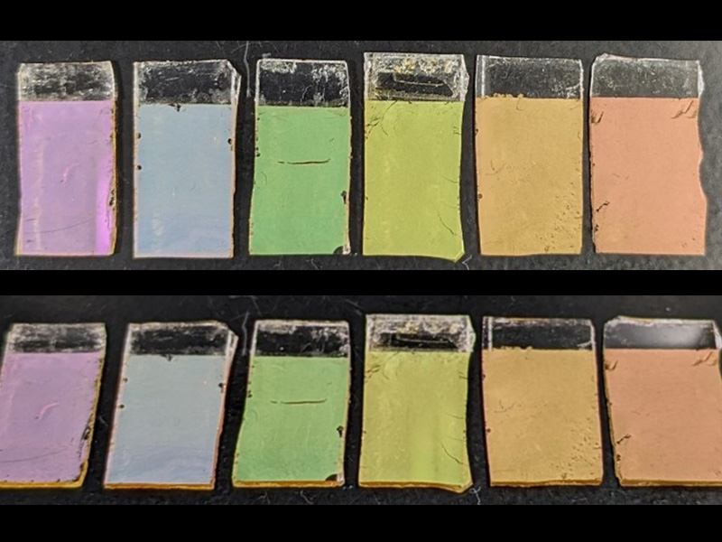
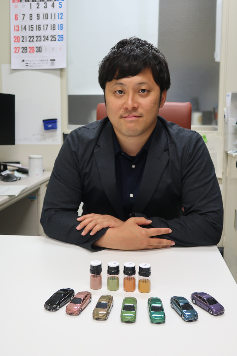
Another change I can mention is that our research results now have the potential to be adopted by society. We don’t just produce research papers and results on the fundamentals of nano-antennas as a Kobe University research group; we also consider how these results can be useful in society. One of these social applications is our “structural color ink.”
Making any color imaginable from a single material ― An idea derived from physics
One application of nanoparticles, structural color ink, was published last year to much acclaim.
Sugimoto:
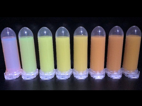
Through a phenomenon known as Mie resonance, by changing the size of silicon nanoparticles, one can freely determine the wavelength and color to which they respond. The idea of using a single material to control light in order to display any color is an idea only possible through physics; an idea that was not possible in the area of general paints, in which materials correspond with colors. Not only that, it is incredibly effective in producing color, resulting in dramatically lower amounts needed to achieve coloration.
Structural color can actually be found on things around us, such as CDs and the wings of jewel beetles. These types of surfaces have microscopic structures that interfere with light to display colors. These structural colors brighten depending on the angle at which they’re viewed, which had previously limited the range of their applications for commercial products. While silicon nanoparticles are also classified as structural colors, these colors can be produced by the particle, which means that the color stays the same no matter which angle you view them from. It was difficult to produce the microscopic structures required for structural color in paint, but since color is produced at the single nanoparticle layer in these silicon nanoparticles, it has become possible to use them in structural color paints and inks.
Another characteristic of structural color paint is that the amount of paint used is extremely small. Since color is expressed even in a single layer of nanoparticles, the thickness of the coat of structural color paint is one-hundredth that of conventional paint. Using this paint on automobiles and airplanes will see huge benefits in terms of cost efficiency. The paint is also a resilient material, able to withstand temperatures of 500 ºC.
What about some applications of structural color ink?
Sugimoto:
Some obvious applications are for printing and film, but it’s actually possible to apply this ink to cosmetics as well. In addition to only requiring a small amount to express color, silicon nanoparticles are also good at concealing surfaces beneath them, making them well-suited for cosmetic products. They’re also safe to apply to the skin and are hypoallergenic, and since the material itself naturally absorbs ultraviolet light, they’re also great at blocking UV rays.
We’ve also heard various proposals for applications from different corporations. Since it’s such a large market, our eventual goal is to apply this technology to paints for automobiles. In fact, we’re currently running a gap fund project in JST’s “Deep tech startup international development program (D-Global).”
The technology behind this structural color ink is also currently being showcased at Expo 2025 Osaka, Kansai in Osaka City.
Are you considering any future development for structural color ink?
Sugimoto:
In JST D-Global, we’re thinking of launching a startup by the end of the fiscal year 2026. Rather than licensing the technology to corporations, we’re aiming to become a manufacturer that can take care of the core processes in-house. Thus, we’ve teamed up with management candidates and gathered powerful allies and are now developing our technology for practical use. On the university side of things, we’re preparing a backup system of talent, including individuals from the Enterprise Partnerships Division. Colors are used in all kinds of products, meaning the market is both broad and very, very large. We’re undergoing preparations to get an idea of whether we can apply what we’ve demonstrated in the laboratory for industrial scale manufacturing.
Accelerating research through development of global talent
What kind of future developments do you see in your research?
Sugimoto:
I’m always thinking about what material will follow silicon in terms of nanoparticle development so that I can take the initiative in my research. But rather than doing something special, I intend to perform thorough research and solidify the science behind this technology so that I can build up the world’s knowledge in the form of research papers.
I’d also like to further advance research and development for structural color ink. I feel that with our nanoparticles, we could even make it so that you don’t even need a single layer of paint to display colors. Theoretically, it’s possible to spread nanoparticles sparsely throughout the ink, making it feasible to be demonstrated at the experimental level. In addition, I hope we can follow this research up by applying it to methods for inkjet printing.
In the best of the best research groups in the USA, the more research you perform, the more outstanding talent will gather to join in. This system leads to the start of new projects and even more talent gathering to join them, which progresses and expands the research. I’m trying to make our research group into a similar organization, so I’m always looking to try new things in order to find new research topics. The various institutions in place in Japan differ from those overseas, making this endeavor somewhat difficult, but I’d like establish a similar system at my research group at Kobe University.
There’s been a noticeable rise in the number of ambitious students, so rather than having one-off researcher exchanges with overseas groups depending on our financial situation, I’d like to construct a system in which we can expand our international joint research efforts though constant researcher exchange with multiple research groups overseas in a stable framework.
Resume
Graduated from the Department of Electrical and Electronic Engineering, Faculty of Engineering, Kobe University in 2012. Completed the master’s program at the Graduate School of Engineering, Kobe University in September 2013. Became visiting scientist at the Boston University Photonics Center in 2014. Completed the doctoral program and received his doctorate in engineering from the Graduate School of Engineering, Kobe University in 2016. Became assistant professor at the Graduate School of Engineering, Kobe University in October 2016. Became associate professor at the Graduate School of Engineering, Kobe University and distinguished associate professor at the Institute for Advanced Research in October 2022.